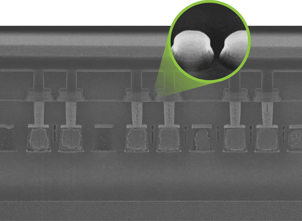
Cross section photos of a semiconductor device are taken using a Scanning Electron Microscope (SEM) or Transmission Electron Microscope (TEM) which are able to capture the individual layers and miniature features of the device.
Cross section photos of a semiconductor device are taken using a Scanning Electron Microscope (SEM) or Transmission Electron Microscope (TEM) which are able to capture the individual layers and miniature features of the device.